Electrified Potential/ Development Bias and Vref Correction are done with the following procedure.
The operation time differs depending on the line speed.
Adjusting the ID sensor Vsg
The machine adjusts the LED strength of the ID sensor so that the value of Vsg (the charge which is detected from the background on the Transfer Belt) will be in the range of 4.0V ±0.5V. When the center ID sensor detects that the Vsg value is not within the target range three times, SC370-02 (ID sensor error) will be issued.
- SP3-320-031/032/033 (Vsg Error Counter)
- SP3-320-013 (Vsg Upper Threshold)
SP3-320-014 (Vsg Lower Threshold)
If Vsg of the front or rear ID sensors fails to reach the target adjustment value, SC370-01/03 (logging SC) is issued. In such a case, the intervals during the process control become shorter and this may result in a longer wait time.
Furthermore, if Vsg<0.3V, SC371-01, SC371-02, or SC371-03 (ID sensor output error: output on the background [specular reflection]) is issued.
If 0.3V≦Vsg≦V2.2V, SC375-01 or SC375-02 (ID sensor output error: damage to the belt detected) is issued.
Agitating the Developer (10 seconds)
The machine agitates the developer and reads the TD sensor output.- SP3-539-001 (Dev Agitating Time :Set)
- Creating patterns, detecting the density
10 patterns are created on the transfer belt and detected by each ID sensor, with the Charge/ Development Bias adjusted for each pattern.
The ID sensor contains an LED [B] and two types of photodetectors. The sensor detects the reflection from the LED with the positive photodetector (REG) [A] and the diffusion photodetector (DIF) [C].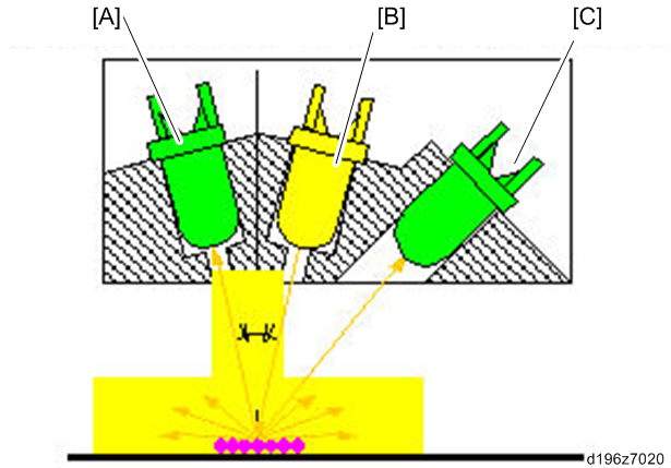
- Determining Vtref from the Development Gamma
This decides the charge voltage and development bias